
Introduction
The term computer comes from the word “computing” and refers to the powerful processing capabilities of the processors. However, the computing power is just a subset of the functionalities provided by computers. To leverage all this computing power, one has to load an operating system or generally software that performs the computing operations. The software has to be stored somewhere. Usually, storage is realized in the form of disks. Communication and data exchange with those disks is typically standardized. There are many communication buses in modern systems, such as SATA, USB, and PCI Express etc. All of them serve a common purpose - the data exchange between the processor and the peripheral. Furthermore, we can call them I/O (input/output) buses, because they can often be used by humans for interacting with the computer.
Initializing a modern computer, i.e., preparing it to run software or an operating system, is a job for the firmware - the lowest-level code that does processor-specific initialization. The firmware not only needs to initialize the computing units (CPUs) but also the I/O buses. CPUs by themselves are not so usable without input/output from humans. In this blog post, I will explain how I/O buses can be initialized on modern server systems based on the AMD Turin processor family and the Gigabyte MZ33-AR1.
We also have other blog posts describing the efforts of porting the Gigabyte MZ33-AR1. I encourage you to read them in case you have missed some.
Port mapping
SATA and USB buses have been available in every PC for many years. SATA was the main disk bus until it was superseded by PCI Express-connected NVMe drives. However, it may still be frequently used in NAS or any other RAID matrices. USB, on the other hand, is more universal and allows connecting a variety of device types, from small storage (USB drives), to human input devices like: keyboards, mice, fingerprint sensors, microphones, speakers, cameras, and HSMs. One could say that these two buses (SATA and USB) are the most crucial ones to create a human-usable PC. We should also include the display, of course, for completeness; however, the display is not the subject of this blog post.
The Gigabyte MZ33-AR1 board offers up to 16 SATA ports, two rear panel USB 3.x
ports, two front panel USB3.x ports on internal F_USB3 header, and two front
panel USB2.0 ports on internal F_USB2 header. You may check the board
manual
for details. We know how many ports we have, but we don’t know how they are
routed to the SoC. Without that knowledge, we can’t add a proper configuration
of those ports to coreboot. That’s where the port mapping comes into play.
The easiest way to do a port mapping is to plug a drive into each port of each bus and see where they pop up in the operating system. We will use generic Linux system utilities to obtain that information:
lsusb- listing USB topology of the ports and devicesdmesg- listing the SATA and USB controllers on PCI domains, detecting which SATA drive is connected to which SATA controller
USB port mapping
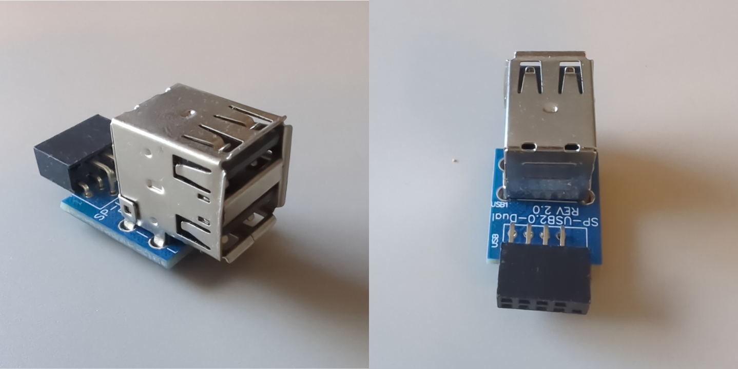
To map USB ports, we just need a Linux distribution installed on the target
system: a USB3.x drive and a USB2.0-only drive. The chassis we use with the
Gigabyte MZ33-AR1 already has two front panel USB3.x ports, which are
connected to F_USB3. We just need an adapter for USB 2.0 ports that will
connect to F_USB2, like this one:
To start the mapping, we have to simply plug both of the drives into each port
and see where they pop up in the lsusb output. Here is an example of the
first round of the mapping:
|
|
From the above, we can see our two drives:
Bus 003 Device 004: ID 048d:1234 Integrated Technology Express, Inc. Chipsbank CBM2199 Flash DriveBus 004 Device 003: ID 0781:5591 SanDisk Corp. Ultra Flair
Besides our drives, we can also see the American Megatrends, Inc. Virtual
devices. These are the devices exposed by the Baseboard Management Controller
(BMC) to provide KVM and remote storage mounting services. We can see that
they are connected through a hub to port 2 of our USB controller:
|
|
We will be seeing these devices on each round of the mapping, so we can skip
looking at them. For now, we have to know that port 002 of the XHCI USB2.0
the controller on bus 001 is occupied by the BMC. We know it is 2.0 because
the speed of the controller is 480M. USB 3.0 controllers and ports have
either 5000M or 10000M, depending on USB3 generation.
Now we have to locate where our USB sticks are on the USB topology. We have to
look at the Bus and Device numbers from the raw lsusb output and match
them with the numbers on lsusb -t output:
|
|
Here we can see that Chipsbank CBM2199 on Bus 003 Device 004 is connected
to USB 2.0 XHCI controller port 001, but it is connected through a hub. So
the port 001 of the CPU USB controller is connected to the USB 2.0 hub (Bus 003 Device 002). In the lsusb output, we can see it is: Bus 003 Device 002: ID 0bda:5411 Realtek Semiconductor Corp. RTS5411 Hub.
Next step is to swap the drives with each other to test USB 2.0 and USB3.x in the very same port, and then move to the next pair of ports, repeat the same mapping steps as above, until we exhaust all options. It is important to keep a record of where we plugged each driver, so we know which port it maps to physically. And so after all rounds of plugging the drives, we obtained the following map:
- Bus 1 - XHCI USB 2.0 controller root hub:
- port1: Realtek RTS5411 hub
- hub port 1: rear USB 3.x port bottom
- hub port 2: rear USB 3.x port top
- hub port 3:
F_USB2 - hub port 4:
F_USB2
- port2: BMC hub
- port1: Realtek RTS5411 hub
- Bus 2 - XHCI USB 3.x controller root hub:
- port 1: Realtek hub
- hub port1: rear USB 3.x port bottom
- hub port2: rear USB 3.x port top
- port 1: Realtek hub
- Bus 3: XHCI USB 2.0 controller root hub:
- port 1: Realtek RTS5411 hub
- hub port1:
F_USB3 - hub port2:
F_USB3
- hub port1:
- port 1: Realtek RTS5411 hub
- Bus 3: XHCI USB 3.x controller root hub:
- port 1: Realtek hub
- hub port1:
F_USB3 - hub port2:
F_USB3
- hub port1:
- port 1: Realtek hub
This is the complete map of the USB ports as seen by the OS. If we look at the board manual, we will see the same topology on the block diagram:
Although the rear USB3.x ports should not be connected through the Realtek hub according to the diagram, the reality is different.
The last thing to do is to check which PCI devices the USB controllers correspond to. This can be done with dmesg:
|
|
So now we have the following mapping:
- PCI
0000:e1:00.4- XHCI controller for USB bus 1 and 2 - PCI
0000:42:00.4- XHCI controller for USB bus 3 and 4
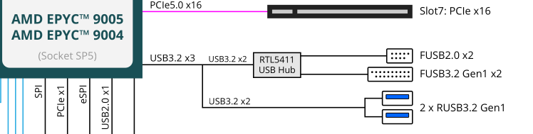
Why are there multiple XHCI controllers, one may ask? Well, we would have to dive into the Turin CPU architecture a bit to understand the PCI domain layout. We will also need this understanding to map the SATA controllers and ports to the actual physical connections to the CPU. But we will dive into that a little bit later in the post.
SATA port mapping
SATA ports on the Gigabyte MZ33-AR1 are exposed on the MCIO connectors. These connectors are typically used on servers and are rather unlikely to be found on consumer/client boards. According to the board manual, SATA ports can be found on the following connectors:
U2_P0_G3A- MCIO Connector (PCle Gen5/SATA)U2_P0_G3B- MCIO Connector (PCle Gen5/SATA)
To connect the SATA disks to these MCIO connectors, we will need an MCIO to SATA x8 cable. Fortunately, such a cable comes in a bundle with the Gigabyte MZ33-AR1 mainboard. To power the SATA drives, we simply need the power cables from the ATX power supply bundle. As the SATA ports are not configured as hot-pluggable, we have to reboot the system each time to obtain the mapping after changing the connected disks (safest). There is a possibility to rescan the SCSI hosts to make the drivers rescan the drives:
|
|
We can see that 4 SATA controllers are mapped to SCSI hosts 0-17:
- PCI
0000:e2:00.0SATA controller - ata1 (SCSI host0) - PCI
0000:e2:00.1SATA controller - ata2 (SCSI host1) - PCI
0000:43:00.0SATA controller - ata3-10 (SCSI hosts 2-9) - PCI
0000:43:00.1SATA controller - ata11-18 (SCSI hosts 10-17)
To invoke the rescan of these SCSI hosts, we can use the following command each time we swap disk connections:
|
|
So let’s start with U2_P0_G3A MCIO. We will use the dmesg output to understand
the mapping of SATA ports:
|
|
I had three disks at hand to use:
- Samsung SSD 870 EVO 1TB
- TOSHIBA-TR200
- ST1000LM048-2E7172
And I connected them to P0, P1, and P2 on the MCIO to SATA x8 cable. We can
see that the disks appeared in ascending order on ata3/4/5 respectively. We
can already notice that the 8 SATA ports on U2_P0_G3A will map to the
ata3-9, so the PCI 0000:43:00.0 SATA controller. Now, let’s move the MCIO
cable to the U2_P0_G3B connector, rescan and gather dmesg output:
|
|
Now we have to look at the later timestamps after we swapped the connector. Now,
we can see the disks appeared at ata11/12/13 respectively. This means the
U2_P0_G3B maps to the PCI 0000:43:00.1 SATA controller.
We still have PCI 0000:e2:00.0 and PCI 0000:e2:00.1 SATA controllers left.
However, they seem to be unused, because we have run out of possible ports.
Each SATA controller has eight ports, except for the two controllers, which
have only a single placeholder port.
Now it is time to map these XHCI and SATA controllers to the correct PCI domains in coreboot and find physical mapping to the CPU.
Turin CPU architecture
PCI topology on each Turin CPU is divided into 8 PCI domains with a root
bridge in each domain. This can be seen clearly with lspci output:
|
|
We can see our SATA and USB controllers in domains 2 (0000:40) and 7
(0000:e0). The domain numbering is simply ordinal, starting from 0. The
domains are assigned their numbers based on the order of appearance in the PCI
enumeration (also the topology shown above). This is how the coreboot’s PCI
device tree has been created for Turin in this
patch.
We should already know from the SATA and USB mapping that the board code should enable the following devices:
- PCI domain 2:
xhci_0sata_2_0sata_2_1
- PCI domain 7:
xhci_1
This has been done in the initial board support
patch, where we already
replicate enabling most of the visible PCI devices in lspci output from the
vendor BIOS. But, is that everything we need? For USB, possibly yes, but not
for SATA. SATA ports are considered high-speed lanes, and they are multiplexed
with PCI Express and CXL (Compute Express Link) lanes on AMD CPUs. In order to
initialize the high-speed lanes for the SATA bus, we have to explicitly define
them as SATA and provide physical lane numbers to initialize them as SATA.
These can be done in MPIO structures, which have been added in the subsequent
patch.
But the question arises - how to get the physical lane numbers? To answer that question we have to understand the physical organization of the I/O lanes in the Turin processor.
SERDES organization
SERDES stands for Serializer/Deserializer, and we can define it as a physical layer for PCIe packet transport, in very simple terms. I will try to explain the organization of the lanes and how they map to the PCI devices/controllers on the Turin systems based on AMD Turin architecture whitepaper.
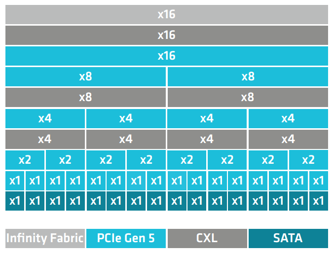
To visualize a SERDES, we can view it as a set of 128 physical lanes that can be configured for different bus types. They are grouped by 16 lanes, providing multiple bifurcation options:
PCIe Gen5, CXL, and SATA are the typical I/O buses used to connect the peripherals to the system. While Infinity Fabric (also called xGMI/GMI link) is a specialized AMD bus to interconnect CPUs on a multi-socket system. This is shown in the figure below:
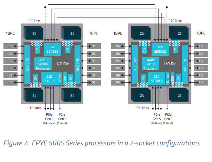
The Turin CPUs have two types of SERDES:
- with “P” links (only 2 x16 groups support xGMI/GMI)
- with “G” links (all x16 groups support xGMI/GMI)
As the figure above shows, 4 x16 groups of “G” links are usually used to interconnect CPUs in a multi-socket system, while “P” links offer I/O extensions. However, in single socket systems, “G” links may be used as an I/O extension too:
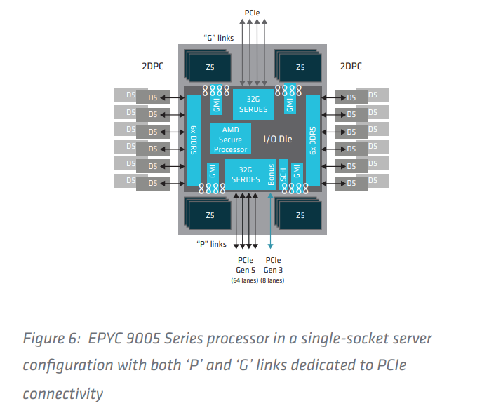
This gives a large number of physical lanes at the board designer’s disposal. The number of available lanes and their possible designation is shown in the table below:
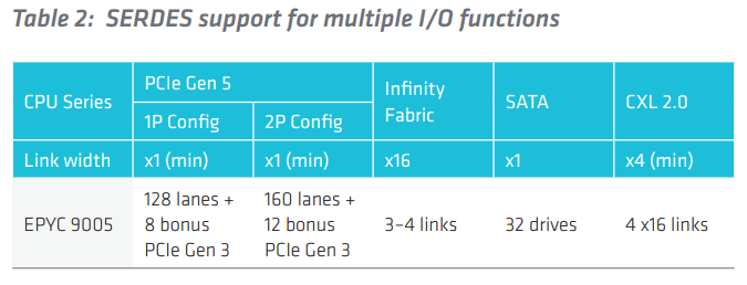
We can also see that there are bonus lanes with lower PCIe speeds for connections that don’t require high bandwidth, e.g., BMC.
Now that we have some basic overview of the architecture, we have to understand how these link types map to PCI domains and how they translate to the physical lanes. It is important to understand that the Turin CPU is divided into 4 NUMAs (Non-Uniform Memory Access):
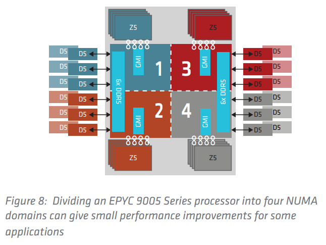
As each processor has 2x SERDES, each SERDES is shared between two NUMA domains. And each NUMA domain consists of 2 PCI domains (4 x NUMA x 2 PCI domains = 8 PCI domains per CPU). So each NUMA domain has a “half” SERDES with “P” and “G” links. These links are simply called P0-P3 and G0-G3, and they correspond to the NUMA numbers:
- NUMA1 - P0 and G0 links
- NUMA2 - P1 and G1 links
- NUMA3 - P2 and G2 links
- NUMA4 - P3 and G3 links
There are also bonus and WAFL links called P4 and P5 (outside of SERDES), which would belong to one of those NUMAs. This is just an ideological division. If I were to be precise, I should use NBIO (Northbridge I/O) and IOHC (I/O Hub Controller) terms, like this:
- NBIO0 IOHC0 - P0 link
- NBIO0 IOHC1 - G1 link
- NBIO0 IOHC2 - P4, P5 and G0 link
- NBIO0 IOHC3 - P1 link
- NBIO1 IOHC0 - P2 link
- NBIO1 IOHC1 - G3 link
- NBIO1 IOHC2 - G2 link
- NBIO1 IOHC3 - P3 link
This mapping is probably more accurate and reflects the 8 PCI domains; however, it is much more confusing, right? For simplicity, I will replace the NBIO and IOHC with the proper PCI domain number. This mapping can be only found in AMD documentation, but with enough probing and poking around, one can derive the mapping themselves. Although I don’t recommend it, it is a tedious process. So the mapping of links to PCI domains is as follows:
- PCI domain 7 - P0 link
- PCI domain 4 - G1 link
- PCI domain 5 - P4, P5 and G0 link
- PCI domain 6 - P1 link
- PCI domain 0 - P2 link
- PCI domain 1 - G3 link
- PCI domain 2 - G2 link
- PCI domain 3 - P3 link
I deliberately did not sort the list in ascending domain order to visualize the oddity of the topology. This oddity has been spotted earlier, and I tried to explain it in this patch (also mentioned it in a previous blog post). This helped me derive the IOHC map for Turin in this patch.
If we look at the link names and numbers, we can see a clear resemblance to the physical connector on the Gigabyte M33-AR1 in the board manual:
U2_P0_G2A(PCle Gen5) —> G2 link lower 8 lanes in x16 groupU2_P0_G3A(PCle Gen5/SATA) —> G3 link lower 8 lanes in x16 groupU2_P0_G3B(PCle Gen5/SATA) —> G3 link higher 8 lanes in x16 groupU2_P0_G0A(PCle Gen5) —> G0 link lower 8 lanes in x16 groupU2_P0_G0B(PCle Gen5) —> G0 link higher 8 lanes in x16 groupU2_P0_G1B(PCle Gen4) —> G1 link higher 8 lanes in x16 group
Unfortunately, there is no mapping of PCIe slots to links in the board manual. Mapping the other MCIO and PCIe devices will require special cables and adapters to confirm the mapping. But PCI Express mapping will be done in the next phase of the project. Right now, it is important to note that our SATA ports are connected to the G3 link.
All we are missing right now is the physical lane numbers, which correspond to the G3 link. The physical lane mapping to the links is fixed in the hardware. Unfortunately, there is no public information about the mapping, nor can it be easily derived by poking the hardware (currently, I am not aware of any method using Linux utilities). The physical lane mapping to the links can be found in the AMD documents. The G3 link has a fixed mapping to lanes 80-95. We can use this to define the start lane number and end lane number in the MPIO structure and mark those lanes as SATA, like this:
|
|
The third information we need to properly initialize the SATA ports is the right GPP bridges that can be used with those physical lanes. Again, the mapping of possible GPP bridges for use with given physical lanes is also explained only in AMD documentation. Since G3 links correspond to the PCI domain 1, we should use the GPP bridges from PCI domain 1 (i.e., PCI device 1 functions 1-7 and PCI device 2 functions 1-2). I decided to use PCI device 2 function 1 and 2 to cleanly separate the SATA port from the PCIe ports that will be added in the near future.
However, something does not seem right… The SATA controllers we wanted to initialize are present in PCI domain 2, but the G3 link is in domain 1… I used the GPP bridges in PCI domain 2 for SATA ports, because that’s where the SATA controller is located. This may be another oddity of the AMD CPU architecture I may not be aware of. Unfortunately, I have no way to test the code, because of this issue. The CPU gets stuck in a loop waiting for another thread to initialize. To prove that SATA and USB work; I would have to be able to boot to the UEFI payload, so that SATA and XHCI USB drivers would enumerate the ports. It seems to be still quite far away from that point.
But the current state can be considered complete, and we have fulfilled the following milestones completely:
- Task 3. Hardware-topology discovery:
-
Milestone a. USB connector map
-
Milestone b. SATA connector map
We have prepared a complete mapping of the USB and SATA ports, as explained in the blog post.
-
The following milestone can be considered as fulfilled partially:
- Task 4. Port configuration in coreboot
-
Milestone a. USB & SATA devicetree descriptors
The initial patch adds the configuration of the SATA and USB controllers. Subsequent patch adds the MPIO descriptors required for SATA ports initialization and updates USB configuration. Unfortunately, we have no way to verify the SATA and USB operation due to issues with early CPU initialization, so this milestone can be considered only half done - code complete.
-
Summary
We have made significant progress in the porting process. We have successfully moved from running just the bootblock to running the OpenSIL already, and attempting to perform the silicon initialization. More exciting stuff is yet to come, so stay tuned for the next blog posts.
Huge kudos to NLnet Foundation for sponsoring the project.
![]()
Unlock the full potential of your hardware and secure your firmware with the
experts at 3mdeb! If you’re looking to boost your product’s performance and
protect it from potential security threats, our team is here to help.
Schedule a call with
us
or drop us an email at contact<at>3mdeb<dot>com to start unlocking the
hidden benefits of your hardware. And if you want to stay up-to-date on all
things firmware security and optimization, be sure to sign up for our Dasharo
newsletter:
