Introduction
Continuing the process of I/O buses initialization from the previous post. In this blog post, I will explain how PCI Express buses can be initialized on modern server systems based on the AMD Turin processor family and the Gigabyte MZ33-AR1.
If you haven’t read previous blog posts, especially the SATA and USB initialization post, I encourage you to read them in case you have missed some. Lots of concepts explained earlier will be used to describe the process of PCI Express initialization.
Mapping of PCI Express ports
Mapping of PCI Express ports to hardware lanes is the prerequisite for porting the configuration to any open-source firmware. While on Intel platforms it is pretty straightforward, each PCI Express root port has its unique PCI device and function, on AMD systems, the matter is a bit more complicated.
Modern AMD systems have multiple SERDES with 16 lanes each. Each SERDES can bifurcate into various configurations to support up to 9 PCI Express root ports, e.g., 1x8 and 8x1. Each bifurcated root port needs an assigned bridge by the BIOS, where the endpoint devices could be enumerated. The assignment of bridges and lanes has to follow a specific set of rules. But before that, let’s try to map the port to hardware lanes.
Before we can approach the mapping, we will need special cables and adapters to populate the PCI Express slots and connectors:
- Dual MCIO(74pin) 8i to PCIe5.0 X16 Gen5 Male Adapter
- Dual MCIO 8i to PCIe5.0 X16 Gen5 female Adapter
- MCIO to MCIO 8i Cable
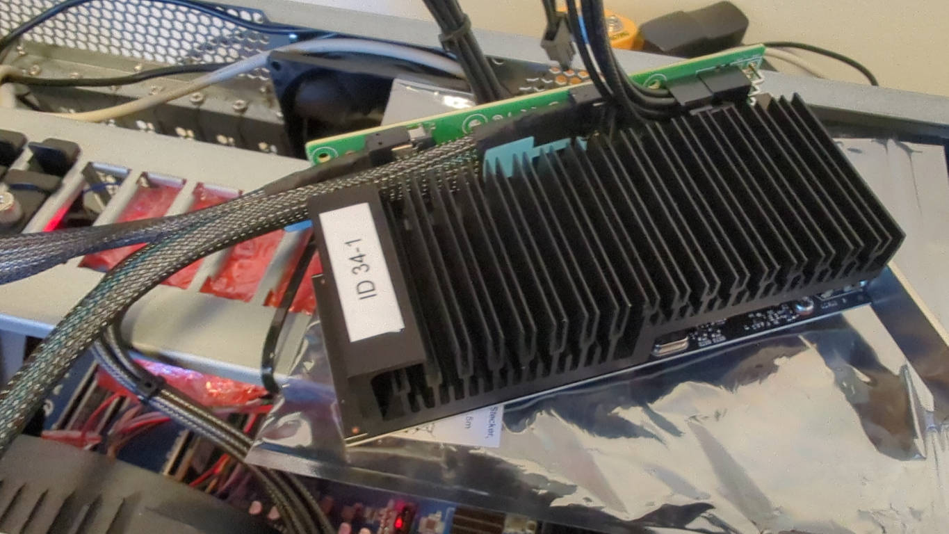
Thanks to these cables and adapters, we will be able to plug regular PCI Express expansion cards. I have used an MSI GeForce GT1030 card in the MCIO 8i to a PCIe5.0 X16 female adapter as an endpoint device.
We will also use the AMD XIO tool for Linux to help with the mapping. This utility provided by AMD to its partners is for high-speed PHY diagnostic purposes. It is able to show which SERDES and ports the given bridge uses. So without any device populated in the PCI Express or MCIO slots yet, we get the following output:
|
|
The tool gives us the PCI address of the bridge, the SERDES, and its port.
Pretty much everything we need. Unfortunately, the Logical to SERDES Lane
and Logical to Controller Lane are empty, but I hoped it could also give us
some useful information about lane mapping. If the information is not present,
we will have to find that information via other means.
By looking at lspci -tvvnn output, we can match the bridges to the devices
they connect to:
|
|
So we already see that:
- G2 port 0 with four lanes maps to an on-board M.2 slot with the NVMe disk
- P5 port 0 with four lanes maps to the on-board Ethernet devices
- P5 port 2 with one lane maps to the BMC PCI Express link for VGA
When the GT1030 card was plugged into the PCIE_3 slot via the adapters and
cable, a new bridge appeared in the AMD XIO output:
|
|
We see that PCIE_3 slot maps to P0. The port number can be ignored since the
slot has to occupy all 16 lanes. Now, when connecting the GPU to the MCIO
connector, e.g., U2_P0_G3B, we get the following output:
|
|
Judging from above, we deduce that U2_P0_G3B maps to G3 port 2 and higher.
Because the MCIO connector has eight lanes, but the GPU uses only four, the G3
port 3 is currently not occupied. It is also important to note that the
Gigabyte BIOS supports only x4x4 bifurcation of the MCIO connectors. So all
devices appearing in these MCIO connectors will always occupy only one of two
ports on the given SERDES.
To complete the mapping, we have to plug our GPU into all possible PCIe slots and MCIO connectors and gather the results. I have gathered full mapping results from AMD XIO for the reference here.
In short, we have the following map:
- G2 port 0 with four lanes maps to an on-board M.2 slot with the NVMe disk
- P5 port 0 with four lanes maps to on-board Ethernet devices
- P5 port 2 with one lane maps to the BMC PCI Express link for VGA
- G2 port 2 with four lanes maps to
U2_P0_G2AMCIO connector (another four lanes got G2 port 3 as well, lanes are reversed) - G0 port 3 with four lanes maps to
U2_P0_G0AMCIO connector (another four lanes got G0 port 2 as well, lanes are reversed) - G0 port 1 with four lanes maps to
U2_P0_G0BMCIO connector (another four lanes got G0 port 0 as well, lanes are reversed) - G3 port 2 with four lanes maps to
U2_P0_G3BMCIO connector (another four lanes got G3 port 3 as well) - G3 port 0 with four lanes maps to
U2_P0_G3AMCIO connector (another four lanes got G0 port 1 as well) - P3 port 1 with 4 lanes map to
PCIE_7(each 4 lanes map to P3 port 0/1/2/3 respectively) - P2 port 2 with 4 lanes map to
PCIE_6(each 4 lanes map to P2 port 0/1/2/3 respectively) - P1 port 2 with 4 lanes map to
PCIE_4(each 4 lanes map to P2 port 0/1/2/3 respectively) - P0 port 2 with 4 lanes map to
PCIE_3(each 4 lanes map to P1 port 0/1/2/3 respectively)
By switching the cables when mapping PCIE_n ports, we can get different
results due to lane swapping. Also, some of the ports are internally reversed,
which is why the devices appear on different SERDES ports.
The above map fulfills the following milestone:
- Task 3. Hardware-topology discovery - Milestone c. PCIe lane map
You may already see how complicated it gets once the lane reversals and cable swapping come into play. We will demystify it in the next step, which is PCI Express port configuration.
PCI Express configuration
Now that the mapping is complete, we can start configuring the slots and
connectors. We will do it in a similar fashion as for SATA, but we of course
need to change the interface type from SATA to PCIE. During the mapping, I
mentioned that we miss the Logical to SERDES Lane and Logical to Controller Lane information. Thankfully, we can find that information in the OpenSIL
code
itself:
|
|
These arrays tell us which ports are internally reversed in hardware and what the starting lanes are. This is enough to write down the code we need to initialize the ports. Well, almost… There is a set of rules explained in the AMD documentation one has to follow to allocate PCIe bridges properly:
- Bridges should be allocated starting with the port with the widest link
- The lane numbers should be assigned to bridges in ascending order, except for reversed links
- For reversed links, the bridges should use descending lane numbers, e.g., for P3 the ports should start from 31 down to 16
- If P4 and P5 links have the same width, prioritize P5
- P4/P5 links have lane numbers 128-135
- WAFL links can only be on lanes 132 and 133 and occupy a function
- Lane reversal is handled in the opposite order
- Each bridge of G0-3 and P0-3 can only be allocated to PCI addresses 1.1-1.7 and 2.1-2.2 (up to 9 root ports)
- Bridges of P4/P5 links can only be allocated to PCI addresses 3.1-3.7 and 4.1 (up to 8 root ports)
From the previous post, we know that:
- PCI domain 7 - P0 link
- PCI domain 4 - G1 link
- PCI domain 5 - P4, P5 and G0 link
- PCI domain 6 - P1 link
- PCI domain 0 - P2 link
- PCI domain 1 - G3 link
- PCI domain 2 - G2 link
- PCI domain 3 - P3 link
With that in mind, we can easily prepare the lane numbers and the PCI device addresses for all the slots and connectors:
- M.2 NVMe G2 port 0 -> domain 2 device 1.1, 4 lanes from the
start of G0:
- start lane 112
- end lane 115
- Ethernet P5 port 0 -> domain 5 device 3.1, 4 lanes from the
start of P5:
- start lane 128
- end lane 131
- BMC VGA P5 port 2 -> this is tricky, there is a gap between Ethernet and BMC
VGA, so the start lane number for VGA may be only 134, because WAFL links
are at lanes 132-133 and occupy a function, so BMC VGA will be at domain 5
device 3.3, 6th lane from the start:
- start lane 134
- end lane 134
U2_P0_G2AG2 x4x4 -> domain 2 devices 1.3 and 1.4, eight lanes from the middle of G2, four lanes per device:- start lane 120 and 124 respectively
- end lane 123 and 127 respectively
U2_P0_G0AG0 x4x4 -> domain 2 devices 1.1 and 1.2. 8 lanes from the middle of G0, because the core is reversed, four lanes per device:- start lane 108 and 104 respectively
- end lane 111 and 107 respectively
U2_P0_G0BG0 x4x4 -> domain 2 devices 1.2 and 1.1. 8 lanes from the start of G0, because the core is reversed, four lanes per device:- start lane 100 and 96 respectively
- end lane 103 and 99 respectively
U2_P0_G3AandU2_P0_G3Bare already configured for SATA, thus skipping them. If they were to be configured as PCI Express, then the code should allocate lanes 80-95 (four lanes each port) for PCIe on bridges 1.1-1.4 on domain 3 (not domain 1 as written above, apparently the P3 and G3 are swapped and after initialization, the root bridges appear in different PCI domains)PCIE_7P3 x4x4x4x4 -> domain 1 (not domain 3, mind the swap) devices 1.1-1.4, 4 lanes each device, core reversed:- start lane 28, 24, 20, 16 respectively
- end lane 31, 27, 23, 19 respectively
PCIE_6P2 x4x4x4x4 -> domain 0 devices 1.1-1.4, 4 lanes each device, core reversed:- start lane 60, 56, 52, 48 respectively
- end lane 63, 59, 55, 51 respectively
PCIE_4P1 x4x4x4x4 -> domain 6 devices 1.1-1.4, 4 lanes each device:- start lane 32, 36, 40, 44 respectively
- end lane 35, 39, 43, 47 respectively
PCIE_3P0 x4x4x4x4 -> domain 7 devices 1.1-1.4, 4 lanes each device:- start lane 0, 4, 8, 12 respectively
- end lane 3, 7, 11, 15 respectively
The patches that initialize those ports with the above lane numbers are linked below:
PCIe validation
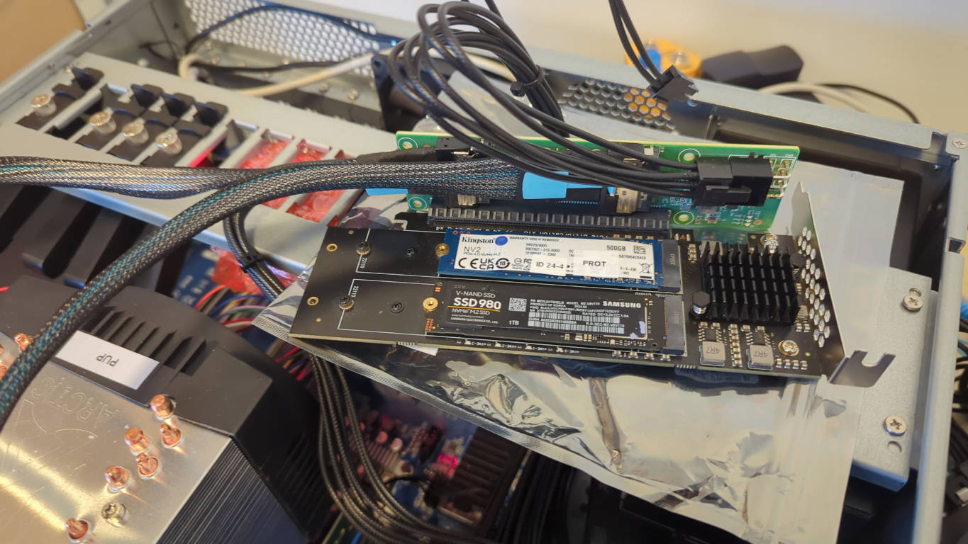
Now that we have the PCIe configuration coded, it’s time to validate if it works properly. To validate every possible port described in the coreboot’s devicetree, we will be using another adapter, this time a PCIe x16 to 4x NVMe M.2 slot:
We will be plugging four different disks into this adapter and then plugging it into every MCIO and PCIe slot to check if the disks appear in the firmware and possibly work in the operating system. For the past few weeks, we have been intensively working to get some operating system booting, and we finally succeeded in running Xen on top of a Linux distribution. Unfortunately, bare metal Linux still faces problems during CPU bring-up due to spurious interrupts happening during AP wake, causing the memory to be corrupted. On the day of writing this post, there are over 60 patches porting support of the Turin processor family and fixing various bugs in coreboot. We will be going through those patches in subsequent posts while explaining the fulfillment of other milestones.
But let’s get back to PCIe testing. We have four different NVMe disks:
- KINGSTON SKC3000S512G (actually two of them, one in the on-board M.2 slot, second in the adapter)
- KINGSTON SNV2S500G
- Samsung SSD 980 1TB
- GIGABYTE GP-GSM2NE3256GNTD
To test whether the disks work in firmware, I simply checked if they appear in
the boot menu (of course, they need to have an EFI partition present with a
bootable OS bootloader for that to work). And in the first PCIE_3 we got:
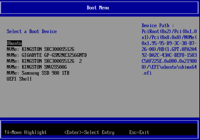
By the way, this picture is done with the BMC KVM VGA opened in the BMC management console GUI, which proves that BMC VGA works. The firmware also accepts virtual keyboard input from BMC, because I could freely browse the setup menu. And here is a sample image from booting Qubes OS:
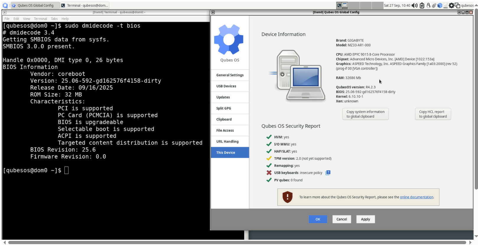
However, for validation purposes, it is easier to boot Ubuntu with Xen hypervisor. I have checked the lspci output to see whether the disks are detected (also on-board devices as well):
|
|
In the above output, we see that all internal devices and all our disks are
detected. To check whether Ethernet actually works, I have pinged
https://nlnet.nl/. If the IP address has been assigned and ping works, then
it means the interface is functional:
|
|
Of course, it wouldn’t be possible without work-in-progress patches with PCI interrupt routing and many others, so keep it in mind. We merely validate whether the physical layer of the PCIe initialization is done properly by OpenSIL.
Additionally, to validate whether the disks are working as well, I used
fdisk to list the partitions on the disks. If the partitions are visible,
then it means the disks are working properly (one of the disks was actually
empty, fresh from the box):
|
|
We have to repeat this test for all possible slots and connectors. The full
validation output from lspci and fdisk for all slots and connectors is
available
here.
This concludes the PCIe initialization, which fulfills the following milestones:
- Task 4. Port configuration in coreboot - Milestone b. PCIe devicetree descriptors
- Task 5. Platform-feature enablement - Milestone b. BMC VGA enablement
- Task 5. Platform-feature enablement - Milestone c. BMC KVM enablement
HCL and data dumping improvements on AMD systems
In the early phases of porting the Gigabyte MZ33-AR1 board, we have improved PSPTool to be able to parse Zen5 images and be able to construct the blobs properly to build a bootable image. We are further improving the parsing with a couple of bug fixes and displaying additional information about the images. In short, we have added proper distinguishing of the blobs of the same type but for different CPU variants by displaying the instance and subprogram fields. These fields, along with the type, uniquely define the purpose of the binary. Previously, the tool assumed that the type is longer than 8 bits and included the subprogram fields in the type parsing, which was not correct. Additionally, we fixed displaying APOB binaries, which were assumed to be duplicates due to not having any size or offset in flash. As a bonus, we also implemented parsing the microcode files to display their patch level and release date. It should help discover and analyze how vendors care about security by updating the microcode in their firmware images. Sample output of the improved PSPTool parsing the Gigabyte MZ33-AR1 version R11_F08 vendor BIOS image is available here. For more details about the changes, see the commit messages of these two PRs:
The above pull request concludes the planned effort to improve the PSPTool, fulfilling the milestone:
- Task 7. Community tooling contributions - Milestone b. Upstream PSPTool parsing improvements
To assist with porting AMD hardware to coreboot, we also implemented a tool specific to AMD CPUs that dumps useful information for developers. It serves the same purpose as coreboot’s inteltool, but works on AMD systems only, of course. The sources of the tool have been sent to upstream for review and can be found here.
The output of the amdtool -a (dump all possible information) command can be found
here.
This fulfills the milestone:
- Task 7. Community tooling contributions - Milestone c. Introduce amdtool for platform data dumps
However, it would be best to use both PSPTool and amdtool as part of an HCL report. For that purpose, we have integrated these utilities into the Dasharo HCL report.
|
|
A known limitation of stock firmware is that it does not provide access to the internal programmer; therefore, the firmware cannot be dumped. This is why a workaround has been introduced, allowing users to supply their own firmware binaries for HCL analysis. This has been described in DTS documentation.
The status of PSPTool is reported as unknown, due to limitations with the
current tool implementation. PSPTool under most circumstances does not produce
errors, just warnings. Moreover, we established that it returns a success status
when run on Intel firmware binaries, as well as mockup binaries made of zeros.
Despite the returned status, the tool works, which is proven by the logs.
|
|
The logs also showcase that amdtool works.
|
|
The pre-release DTS version with all tools integrated can be downloaded from this link.
This fulfills the milestone:
- Task 7. Community tooling contributions - Milestone a. Integrate PSPTool into coreboot HCL pipeline
Summary
Due to the huge dedication of the team, we are at the stage where we can boot an operating system. This lets us perform the validation more extensively and detect bugs more easily. Of course, there are some bugs still to be solved. More exciting (and complicated) stuff is yet to come, so stay tuned for the next blog posts.
Huge kudos to the NLnet Foundation for sponsoring the project.
![]()
Unlock the full potential of your hardware and secure your firmware with the
experts at 3mdeb! If you’re looking to boost your product’s performance and
protect it from potential security threats, our team is here to help. Schedule
a call with
us or
drop us an email at contact<at>3mdeb<dot>com to start unlocking the hidden
benefits of your hardware. And if you want to stay up-to-date on all things
firmware security and optimization, be sure to sign up for our newsletter: